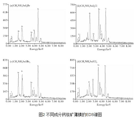
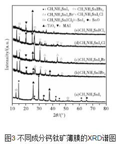
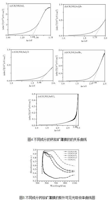
Since the Japanese scholars first studied perovskite-sensitized solar cells in 2009, after five years of development, the photoelectric conversion efficiency of perovskite solar cells has shifted from the initial 3.1% to 19.3%, which has caused great research enthusiasm. Perovskite solar thin-film solar cells have become the focus of people's research. This paper studied the effect of doping of different components on the film-forming performance of tin-perovskite cells, and performed the morphology, phase, absorption and band gap of the thin films. Characterization and testing. The test results show that the perovskite film of CH3NH3SnI3 has the lowest forbidden band width, and its light-absorbing property is superior to other components of perovskite film. The addition of Br and Cl ions results in an increase in the band gap of the perovskite film of the CH3NH3SnI3 composition, and a decrease in the light absorption performance and the crystallization performance. 1 Introduction Organic/inorganic hybrid perovskite solar cells have the characteristics of high energy conversion rate and low processing cost, and have received extensive attention in recent years. The advantage of the organic/inorganic hybrid perovskite material as a solar cell light absorbing layer is that it has excellent bipolar carrier transport properties, and with the replacement or introduction of elements, the energy gap can be within a certain range. Adjustment, while maintaining a stable face-centered cubic structure [1]. At this stage, since the extinction coefficient of the perovskite absorbing layer containing metal Pb is high and the band gap width is appropriate, the research is the most thorough. However, since Pb is harmful to the environment, it would be more environmentally friendly if Pb is replaced by harmless elements. . In recent years, the use of Sn instead of Pb to prepare tin perovskite solar films has been increasing, which is of great significance to explore the preparation of lead-free perovskite solar cells [2]. 2 Preparation of perovskite films with different compositions Fig. 1 shows the SEM morphology of perovskite films with different compositions. The perovskite films of the four components were all obtained after annealing at 100°C for 5 minutes. Compared with the SEM image of CH3NH3SnI3 film (see Fig. 1), when Br- and Cl- are introduced too much, excessive Br- and Cl- may produce some intermediate product during the crystallization, which slows down the perovskite. Crystallization rate, and due to the large atomic size difference between Br-, Cl- and I-, resulting in distortion of the crystal lattice, the crystallization process will be prolonged, and the annealing treatment time also needs to be extended accordingly. Therefore, when the annealing temperature is 100°C, the grain size of the CH3NH3SnIBr2 thin film is not uniform as shown in Fig. 1(c) during a relatively short annealing time of 5 minutes. However, in FIG. 1(d), since the annealing time is short, the crystal grains of the CH3NH3SnICl2 thin film are coarse and the surface of the thin film is not flat and dense. Large cracks appearing on the top of the film in Fig. 6(d) are due to the high voltage at the time of SEM measurement. Figure 2 shows EDS traces of four different composition films, which qualitatively shows the elements contained in the four types of films. Comparing Fig. 2 (a), (C) and Fig. (b) and (d), it can be seen that the relative contents of Br and Cl in the film increase significantly after the addition of excess Br- and Cl-. Since the scan voltage is 20 kV, the radiation penetrates into the TiO2 porous scaffold layer of the perovskite film, resulting in a very high content of Ti in the energy spectrum. FIG. 3 is an XRD spectrum of a five-component perovskite film. It can be seen from FIG. 3 that the five films prepared have a perovskite structure, exhibit good crystallinity, and have a dominant ordered monoclinic crystal orientation. In Fig. 3(a), the diffraction peaks at 2θ of 14.67°, 29.59°, 42.51°, 45.02°, and 61.57° correspond to the (110), (220), (310), (224), and (314) planes, respectively. This shows that the prepared CH3NH3SnI3 has a perovskite structure [3]. The peaks with 2θ of 12.66° and 51.59° respectively correspond to the (001) and (312) crystal planes in the SnI2PDF card, thereby deducing that SnI 2 may be present. Peaks with 2θ of 33.23° and 65.58° respectively correspond to those in the SnO 2 PDF card ( 101), (301) crystal plane, from which it can be inferred that SnO2 may be present. The presence of SnI2 may be due to unreacted raw materials or partial decomposition of CH3NH3SnI2 to SnI2, and SnO2 may be formed by oxidation of CH3NH3SnI2 decomposition products. However, only SnI2 and SnO2 were found in other components, indicating that the doping of Br- and Cl- improves the stability of the crystal to some extent. The diffraction peaks of (b), (c), (d), and (e) in FIG. 3 all shift to high angles because the radius of Br- and Cl- is less than the radius of I-, so that crystals obtained by crystallization are obtained. The lattice constant is relatively reduced, and the diffraction peak shifts toward a high angle. The lines (b) and (c) in FIG. 3 indicate that the diffraction peak shifts toward a high angle as the doping amount of Br- increases. Comparing the lines (b) and (e) in Fig. 3, the diffraction peaks of the perovskite crystals are relatively reduced and the peak intensity is weakened, indicating that the excessive Br-, Cl- incorporation is not conducive to the crystallized film formation of CH3NH3SnI3. The optical band gap has a direct relationship with the light absorption. According to the absorbance spectrum of the sample, the band gap of the five component films is calculated by the Tauc equation extrapolation method. According to semiconductor theory [4], the perovskite film is a direct bandgap semiconductor, so in (1), (2), the light absorption coefficient, A is the absorbance, d is the film thickness, is the Planck constant, 4.13664743 ×10⁻¹⁵eV·s, c is the speed of light, and 2.97982458×10⁸m/s is a numerical value of the wavelength in nanometers, which is the frequency. According to equation (1), equation (2), the abscissa, ordinate, the relationship curve. The intersection of the tangent and abscissa of the curve is the forbidden band width of the film [5]. Figure 4 is a plot of the relationship between different compositions of perovskite films. From Fig. 4(a), the band gap of the film of CH3NH3SnI3 is the smallest, which is 1.44 eV. After the partial doping of Br- and Cl-, as shown in Figures 4(b) and (c), the band gaps of the CH3NH3SnI2Br and CH3NH3SnI2Cl perovskite films increased to 1.75eV and 1.68eV, respectively, due to Br- The introduction of Cl- leads to a decrease in the lattice of the perovskite structure and an increase in the degree of ionization, resulting in a broadening of the band gap. When the doping amount of Br- and Cl- increases, as shown in Fig. 4(d) and (e), the forbidden band widths of the CH3NH3SnIBr2 and CH3NH3SnICl2 perovskite films further increase to 2.08eV and 2.88eV, respectively. Diagram of the relationship between different compositions of perovskite films FIG. 5 is a UV-visible absorption curve of a perovskite film of different composition. As can be seen from FIG. 5, compared with the perovskite film of CH3NH3SnI3 composition, the doping of Br- and Cl- reduces the absorption rate of the perovskite film, and at the same time it absorbs in the visible light range as the doping amount increases. The rate is greatly reduced. Corresponding to Fig. 4(e), the maximum band gap of the CH3NH3SnICl2 perovskite film is 2.88 eV, which results in its low absorption in the visible range. 3 Conclusion The perovskite film of CH3NH3SnI3 has the lowest forbidden band width and reduces its light absorption performance in the visible light range. Excess Br-, Cl- will lead to the decrease of the crystallinity of the perovskite film.
1. Application : For electronical parts
2. Dimension: Customized dimension, OEM & ODM
OD
OD
Tolerance
ID
Tolerance
Roundness
Straightness
Circular
run-out
φ16-20
±0.02
±0.02
0.01↓
0.015↓
0.05↓
φ20-30
±0.02
±0.02
0.01↓
0.015↓
0.05↓
φ30-50
±0.05
±0.05
0.02↓
0.020↓
0.08↓
φ50-80
±0.15
±0.10
0.05↓
0.025↓
0.10↓
7. Trade Terms
Seamless Tube For Electronical Parts Seamless Tube For Electronical Parts,Electronics Aluminum Seamless Tube,Electronics Aluminum Seamless Pipe,Seamless Pipe For Electronical Parts Changzhou YiFei Machinery Co., Ltd. , https://www.yifeialu.com
3.Material: A6063, A6061, A3003
and other series alu alloy
4.Suface
treatment: Anodizing, polishing, turning ,power coating, mill finish
etc
5.Equipment: CNC ,extruding
machine, cold drawn machine, heating oven, straightening machine, cutting
machine
6. STANDARD
PACKING:Wooden case/carton
1. Payment: 30% T/T in advance,
70% balance pay before delivery. L/C at sight.
2. Delivery time: 20 days after deposit receiverd. If opening mould, plus
7-10 days.
3. Trade Term can be chosen depending on your requirements.
4. FOB Port: Shanghai
Research on New Perovskite Solar Cells