With the rise of graphene research, other two-dimensional atomic crystals have also gradually entered the field of research. Among them, hexagonal boron nitride (h-BN) has gradually become another bright spot in the field. The highly similar crystal structure gives h-BN and graphene some common characteristics, such as extremely high in-plane elastic modulus, high temperature stability, and atomic-level smooth surfaces. Because the lattice mismatch between the two is small, the graphene can be evenly and evenly spread on the h-BN substrate. In particular, there are few dangling bonds and charge traps on the h-BN surface, which is beneficial to the reduction of the intrinsic graphene. Extremely high carrier mobility. In addition, h-BN has excellent properties such as wide band gap (5.9 eV), good insulation, chemical stability, and high thermal conductivity, making it an attractive substrate for dielectrics and dielectric materials for graphene-based electronic devices. The preparation method of h-BN two-dimensional atomic crystals is similar to that of graphene. The mechanically exfoliated h-BN has a limited size (several tens of micrometers) and is limited to laboratory research. At present, most studies use chemical vapor deposition (CVD) to prepare h-BN two-dimensional atomic crystals, but the CVD growth process is extremely complicated and various growth parameters are related to each other. In addition, precursors commonly used in CVD methods are highly toxic, have poor stability, are prone to hydrolysis, have many by-products, and are expensive. Therefore, there is an urgent need to develop controllable growth methods for preparing h-BN two-dimensional atomic crystals in other scales. Recently, Zhang Xingwang's research group of the Semiconductor Materials Science Key Laboratory of the Chinese Academy of Sciences has made a series of advances in the preparation of h-BN two-dimensional atomic crystals and graphene/h-BN heterojunctions. Dr. Wang Haolin et al. used ion beam sputter deposition (IBSD) for the first time and used argon ion beam to bombard high-purity h-BN targets. Single and few h-BN two-dimensional atomic crystals were prepared on a copper foil substrate. They found that the introduction of hydrogen during the sputtering process significantly inhibited the nucleation density and produced h-BN single crystal domains with a size of about 5 micrometers. A high-quality continuous film can be obtained by prolonging the growth time. Compared to the widely used CVD method, the IBSD method can precisely control the energy and beam density of the ion beam, and it is easier to achieve controlled growth of the h-BN. In addition, IBSD is a physical vapor deposition method, and the preparation process does not involve chemical reactions. It is expected that h-BN can be directly grown on non-metal substrates, providing a new idea for the preparation of h-BN two-dimensional atomic crystals. The related results were published in Small. 11, 1542 (2015). The small size of crystal domains leads to the existence of a large number of grain boundaries, which will seriously affect the performance of h-BN devices. Therefore, the preparation of large-size single-crystal h-BN has important implications for its properties and device applications. At present, the size of h-BN single crystal domains prepared by most CVD methods is on the order of microns. The team used the IBSD method to treat the substrate by in-situ ion beam etching, and controlled the concentration of sputtered particles on the substrate surface through growth parameters, thereby greatly reducing the nucleation density of h-BN, and ultimately in polycrystalline nickel. H-BN two-dimensional atomic crystals with a single-crystal domain size greater than 100 microns were prepared on a foil substrate. On this basis, the team also prepared a h-BN deep UV prototype detector, the device showed a good UV photoelectric response characteristics. Related results were recently published online at Advanced Materials (DOI: 10.1002/adma.201504042). The graphene/h-BN heterostructure can maintain the extremely high carrier mobility of intrinsic graphene. It is an important basis for the construction of graphene electronic devices and has received extensive attention in recent years. Dr. Meng Junhua and other scientists used CVD technology to grow graphene directly on the IBSD grown h-BN/Cu substrate to prepare graphene/h-BN in-plane and longitudinal laminated heterostructures. By preparing the graphene/h-BN heterostructure by this direct deposition method, it is possible to obtain a large-area, arbitrarily-shaped sample, so that the application of large-area graphene electronics becomes possible; and the introduction of contamination during the transfer process can be avoided. A good graphene/h-BN interface is obtained and the carrier transport performance in graphene is improved. The related results were recently published in Nanoscale 7, 16046 (2015). This study lays the foundation for the preparation of high-quality h-BN two-dimensional atomic crystals, graphene/h-BN heterojunctions and h-BN optoelectronic devices, and will further promote the application of two-dimensional atomic crystals in electronics. The work was funded by the Ministry of Science and Technology, the National Natural Science Foundation of China, and the Beijing Municipal Natural Science Foundation. Polycrystalline Silicon Wafer,Multi Wafer,Polycrystalline Silicon Wafer For Solar Cell,Polycrystalline Solar Cell Wafer ZHONGWEI CITY YINYANG NEW ENERGY , https://www.yinyangnewenergy.com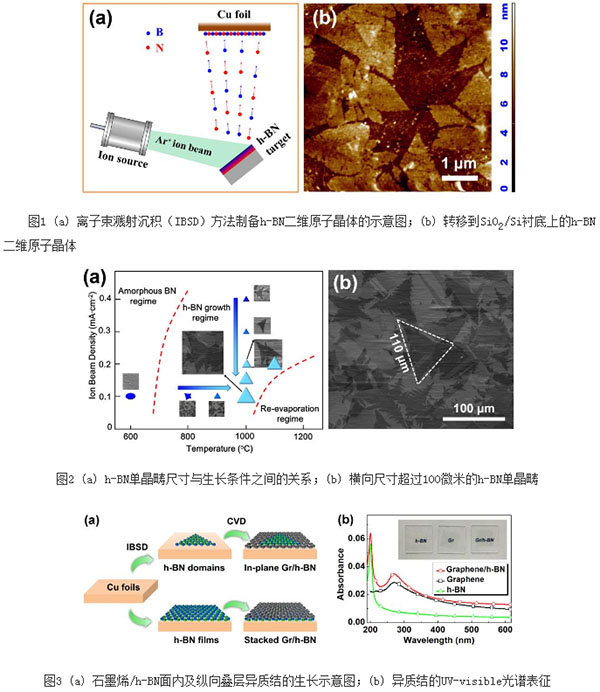
A series of advances in the study of h-BN two-dimensional atomic crystals for semiconductors